
DOUBLE LAYER PCB Manufacturer in India
Reliable Double Layer PCB Manufacturing
Stable. Efficient. Cost-Effective.
High-quality double layer (2 layer) printed circuit boards engineered for reliable electrical performance, stable signal transmission, and consistent manufacturing quality in industrial electronics, automation systems, power supplies, and consumer electronic applications.
- Reliable Electrical Performance
- Stable Signal Transmission
- Ideal for Industrial Electronics
- Cost-Effective PCB Solution
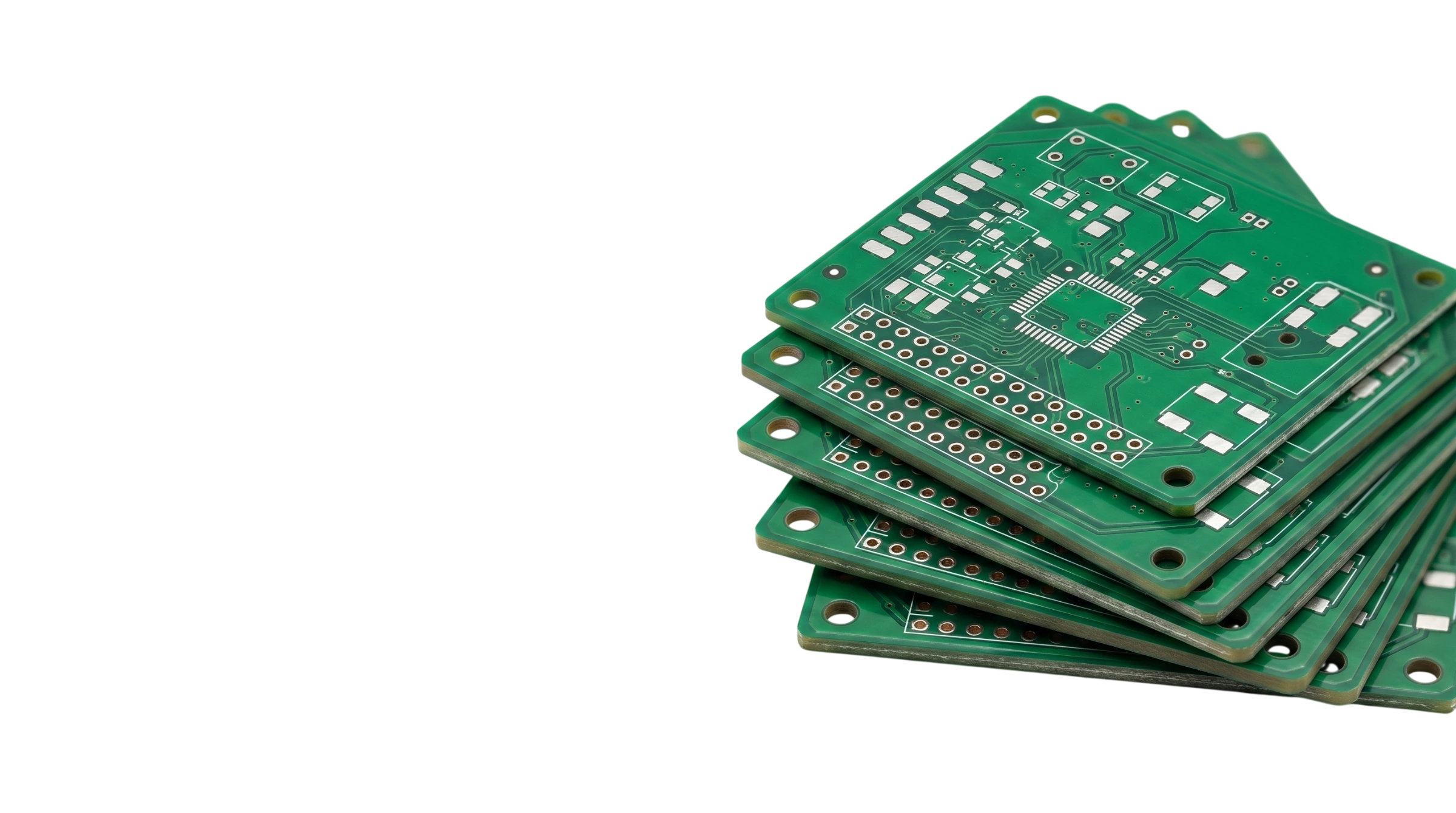
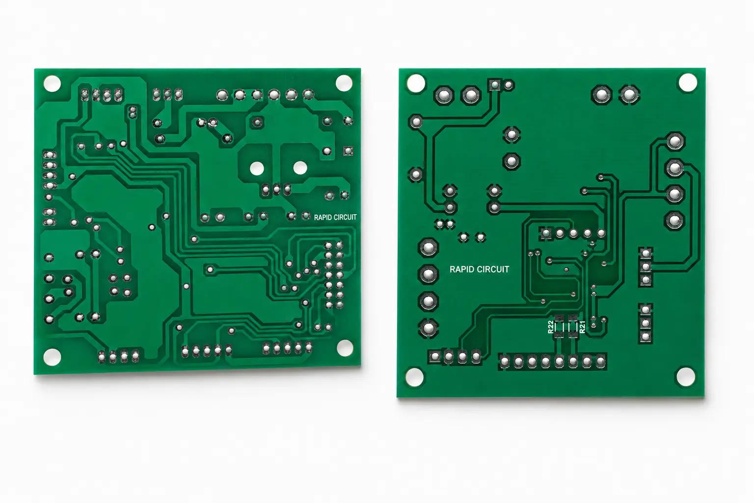
Double Layer PCB
A cost-effective PCB solution for designs requiring two-sided routing, plated-through-hole connectivity, and greater circuit density than single-layer boards.
- Two-sided routing flexibility
- Cost-effective PCB solution
- Higher circuit density than single-layer PCBs
Double Layer PCB Manufacturer in India
If your circuit requires higher complexity and better routing efficiency, choosing a reliable double layer PCB manufacturer is essential. At RAPID CIRCUIT, we provide precision-engineered double-sided PCBs designed for OEMs, industrial applications, and high-performance electronics, ensuring consistent quality from prototype to mass production.
What is a Double Layer PCB?
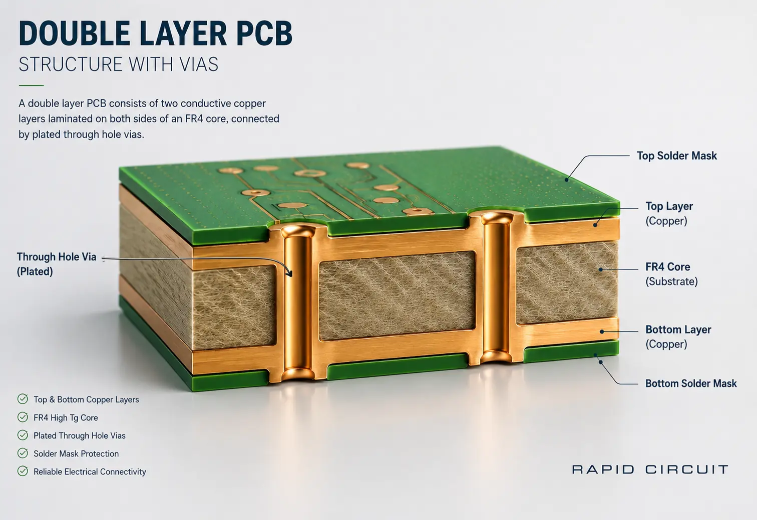
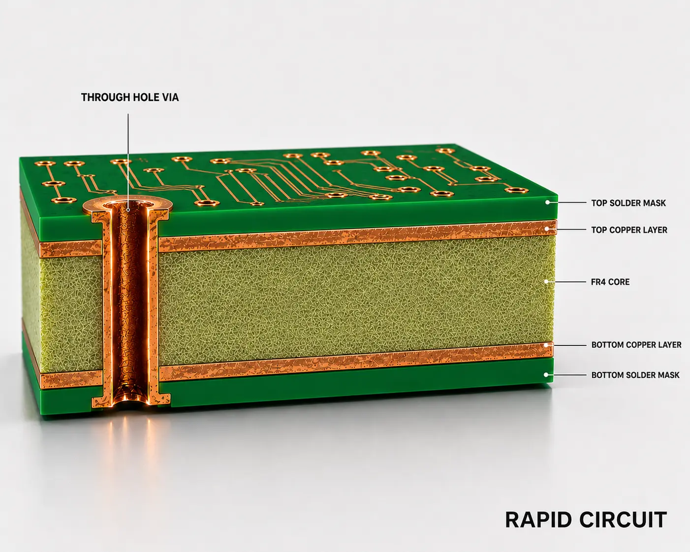
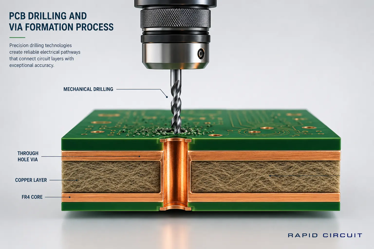
A double layer PCB, also known as a double sided PCB, has conductive copper layers on both sides of the substrate. These layers are connected through plated-through-holes (vias), enabling more complex circuit designs compared to single layer boards.
This structure allows better component density and improved electrical performance.
Technical Specifications of Double Layer PCB
Material
• FR4 (standard)
• High-Tg FR4 (for thermal stability)
• CEM-3
Board Thickness
0.8 mm to 3.2 mm
Copper Weight
• 1 oz (standard)
• 2 oz / 3 oz (heavy copper)
Surface Finish
• HASL (Sn-Pb)
• LF-HASL
• ENIG
• OSP
• Immersion Silver
Minimum Track / Spacing
• 8/8 mil (standard)
• 5/5 mil (minimum manufacturing capability)
• Tighter track and spacing requirements are reviewed based on design and manufacturing feasibility.
Minimum Hole Size
• 0.3 mm (standard)
• Minimum 6 mil (0.15 mm) in special cases
Looking for a reliable double layer PCB supplier?
Get a fast quote with expert engineering support for your project.
Manufacturing Capabilities
• Prototype, small-batch and volume PCB production
• CNC drilling and plated-through-hole (PTH) processing
• Accurate top-to-bottom layer registration
• Gerber file and CAM checks before production
• Quick-turn fabrication for urgent PCB requirements
• Vacuum and moisture-protected packaging for dispatch
Features & Benefits
- Higher circuit density than single layer PCBs
- Improved electrical connectivity
- Reduced board size
- Better signal routing flexibility
- Cost-effective compared to multilayer PCBs
Applications & Industries
Double layer PCBs are widely used in:
• Industrial automation systems
• Automotive electronics
• Power control systems
• Consumer electronics
• Telecom equipment
• Medical devices
Double Layer PCB Manufacturing Process
Step 1: Gerber File Submission
Design files are reviewed for manufacturability.
Step 2 : CAM Processing
Engineering checks include:
• Data Import & Gerber File Verification
• Drill Data Processing (Production Hole Size Optimization)
• Design Rule Check (DRC) for Copper Layers
• Solder Mask & Silkscreen Inspection
• PCB panelization
• Copper Balancing & Thieving for Uniform Plating
• Manufacturing File Generation (Gerber & NC Drill Output)
• Final CAM Inspection & Production Approval
Step 3: Production
• Material Preparation (FR4 Copper-clad Laminate)
• PCB Drilling Process (Via & other PTH drilling)
• Hole Metallization – Plated Through Hole (PTH) Process
• Dry Film Photoresist Lamination
• PCB Imaging & UV Exposure Process
• PCB Developing (Photoresist Development)
• Copper Etching Process (Circuit Formation)
• Solder Mask Application (PCB Protection Layer)
• Silkscreen Printing (Legend & Component Marking)
• PCB Surface Finish (HASL, ENIG, OSP Coating)
• Electrical Testing (Continuity & Short Circuit Test)
• PCB Profiling (Routing, Cutting & V-Scoring)
• Final Inspection, Quality Control & Packaging
Step 4: Quality Control
• Visual inspection
• Dimensional accuracy checks
Step 5: Delivery
Secure packaging with global shipping.
Why Choose RAPID CIRCUIT
Pricing & Cost Factors
The cost of double layer PCB depends on:
- Board complexity
- Number of vias
- Material type
- Copper thickness
- Quantity
- Surface finish
- Lead time
Compared with single-layer PCBs, double-layer boards provide greater routing flexibility and circuit density at a higher manufacturing cost.
Prototype to Production
Support for prototype, small-batch and volume PCB requirements.
CAM Validation
Gerber and manufacturing data are reviewed through CAM processing before production.
Electrical Testing
Electrical testing checks continuity and short circuits before final inspection.
India & Global Delivery
PCB orders can be delivered across India and international markets.
Lead Time / Turnaround
Need a Double Layer PCB Quote?
Submit your PCB files and manufacturing requirements for engineering review and quotation.
Lead times depend on PCB specifications, quantity, material availability, CAM/DFM approval, and current production load. Submit your Gerber files for a confirmed production schedule.
Explore Our PCB Solutions
Double Layer PCB Manufacturing Process steps
Professional manufacturing workflow for 2-layer printed circuit boards used in industrial electronics, automotive systems, communication devices, power supplies, consumer electronics, and advanced electronic applications.
PCB Design & Gerber File Preparation
The 2-layer PCB manufacturing process starts with PCB layout design and Gerber file generation for accurate double-layer PCB fabrication.
Double-Sided Copper Clad Laminate Cutting
Double-sided copper clad laminate materials such as FR4, High-Tg FR4, Rogers, and CEM materials are cut into required production panel sizes.
PCB CNC Drilling
High-precision CNC drilling machines create component holes, via holes, mounting holes, and slot openings according to PCB design data.
Hole Deburring & Surface Cleaning
PCB panels are cleaned and deburred to remove dust, oxidation, resin residue, and drilling burrs before further processing.
PTH Metallization Process
Plated Through Hole (PTH) processing deposits conductive copper inside drilled holes to establish electrical connections between top and bottom layers.
Dry Film Lamination Process
Photosensitive dry film is laminated onto both PCB copper surfaces under controlled temperature and pressure conditions.
PCB Alignment & UV Exposure
PCB artwork films are aligned accurately, and UV exposure transfers the required circuit pattern onto the photoresist layer.
PCB Developing Process
Chemical developing removes unwanted photoresist material and reveals the PCB copper circuit pattern.
Copper Electroplating Process
Additional copper plating increases copper thickness on traces and plated holes for improved conductivity and reliability.
PCB Copper Etching
Unwanted copper is removed through chemical etching, leaving only the required conductive copper circuitry.
Dry Film Stripping Process
Remaining dry film resist material is removed after the etching process to expose clean copper traces.
Solder Mask Coating Process
Protective solder mask coating is applied on both PCB layers to prevent oxidation, solder bridging, and electrical short circuits.
Silkscreen Printing Process
Component markings, polarity symbols, logos, and PCB identification details are printed on the board surface.
PCB Surface Finishing
Surface finishes such as HASL, Lead-Free HASL, ENIG, Immersion Tin, Immersion Silver, or OSP are applied for solderability and copper protection.
PCB Routing & V-Cut Process
Individual PCBs are separated from production panels using CNC routing or V-cut technology.
PCB Electrical Testing
Electrical testing verifies PCB continuity, open circuits, short circuits, and plated hole connectivity between layers.
Final Quality Inspection
Final inspection checks PCB dimensions, copper alignment, solder mask quality, drilling accuracy, and overall manufacturing standards.
PCB Packaging & Dispatch
Finished 2-layer PCBs are vacuum packed or moisture protected for safe transportation and delivery.
Manufacturing Flow
FAQ
What is a Double Layer PCB used for?
It is used in circuits requiring higher complexity, such as industrial systems, automotive
electronics, and telecom devices.
What is the difference between single-layer and double-layer PCBs?
Single layer PCBs have one conductive layer, while double layer PCBs have two layers
connected through vias, allowing more complex designs.
What is the cost of double layer PCB manufacturing?
Costs vary based on complexity, materials, and quantity. Double layer PCBs are slightly
more expensive than single layer but offer better performance.
How long does fabrication take?
Lead time depends on PCB specifications, quantity, material availability, CAM/DFM approval, and current production load. Submit your PCB files for a confirmed manufacturing schedule.
What materials are used?
FR4, High-Tg FR4, Roger and CEM-3 are listed for double-layer PCB manufacturing. Other material requirements are subject to engineering review.
Can I order prototype boards?
Yes, prototype orders are supported before moving to mass production.
Do you provide global shipping?
Yes, PCBs are delivered worldwide with secure packaging.
What files are required for a double-layer PCB quotation?
Submit your PCB files and available manufacturing details, including dimensions, quantity, material, board thickness, copper thickness, surface finish, and delivery requirements.