
Single Layer PCB Manufacturer in India
Single-Sided PCB Manufacturing for Prototype and Production
High-quality single-layer (single-sided) printed circuit boards engineered for economical production, reliable electrical performance, and fast turnaround in consumer electronics, LED lighting, power supplies, and industrial electronic applications.
- Cost-Effective PCB Solution
- Fast PCB Production
- Reliable Electrical Performance
- Ideal for Consumer Electronics
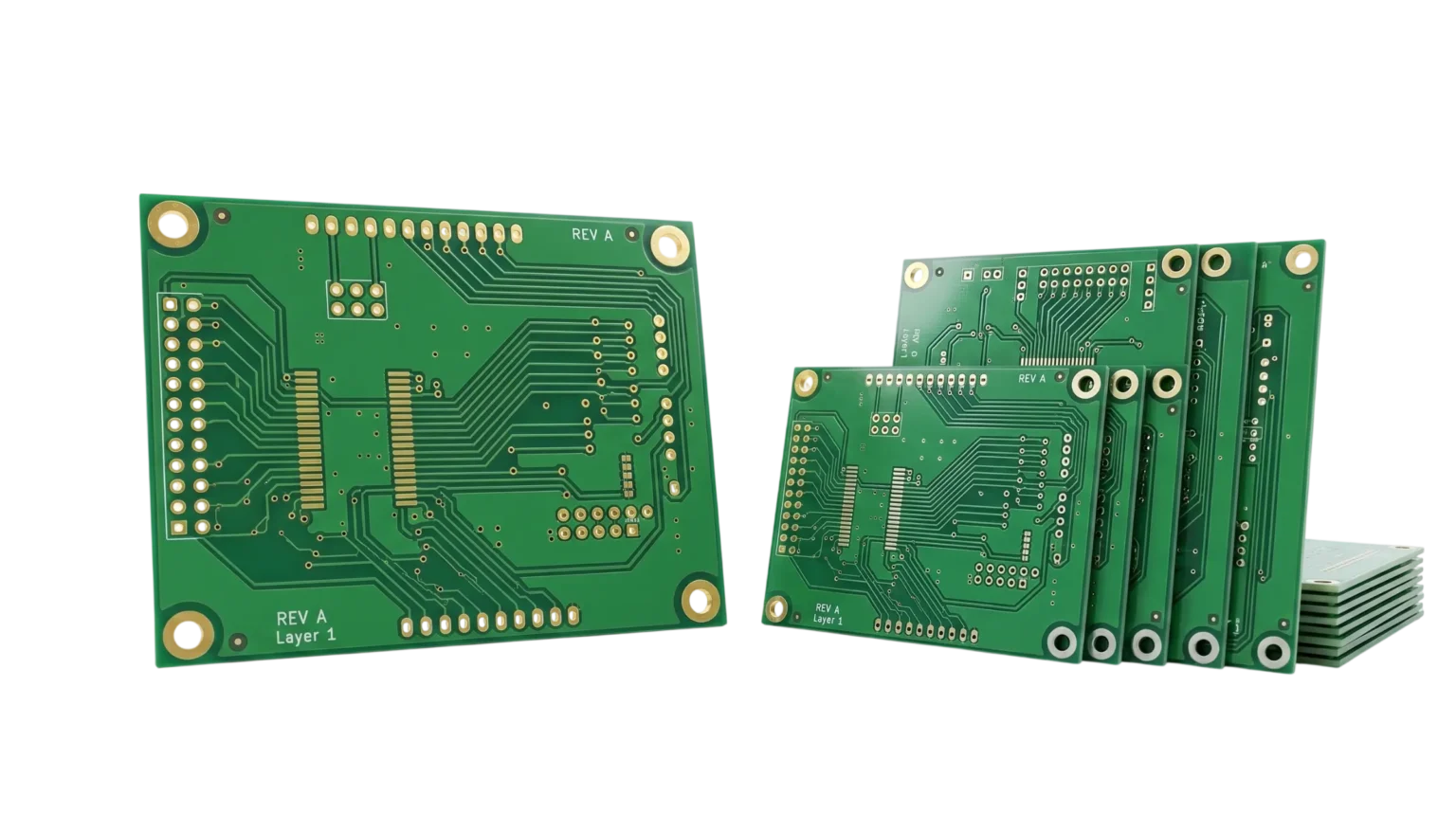
Single Layer PCB Material Options
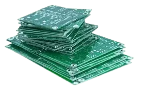
FR4 PCB
Cost-effective single layer PCB ideal for basic electronic applications and bulk production.
- Low Cost
- Suitable for Low Power
- Easy Manufacturing
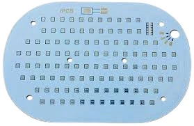
Aluminium PCB
High-performance metal core PCB designed for efficient heat dissipation in high-power applications.
- Excellent Heat Dissipation
- Perfect for LED Boards
- High Thermal Conductivity
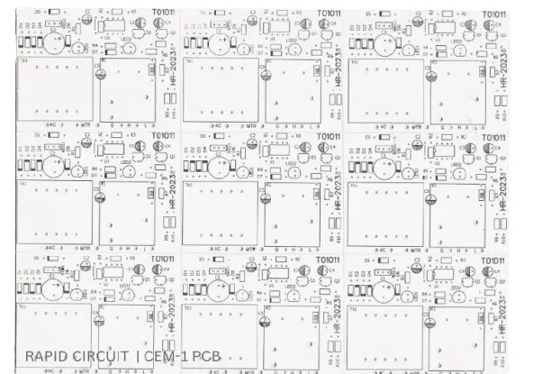
CEM-1 PCB
Reliable composite PCB material offering better strength than FR1 with cost efficiency.
- Stronger than FR1
- Good Electrical Performance
- Moderate Heat Resistance
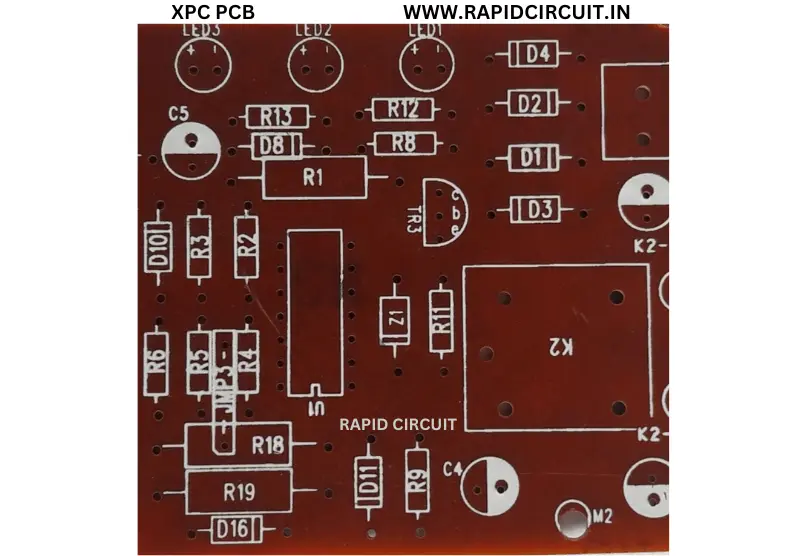
XPC PCB
Durable and flexible PCB material designed for general-purpose electronics.
- Better Heat Resistance
- Strong Structure
- Flexible Material
CEM-3 PCB
High-quality composite PCB with smooth finish and reliable electrical performance.
- Smooth Surface Finish
- Excellent Insulation
- Good Heat Resistance
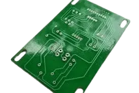
FR1 PCB
Cost-effective single layer PCB ideal for basic electronic applications and mass production.
- Low Cost
- Low Power Applications
- Easy Manufacturing
Single Layer PCB
Looking for a reliable single-layer PCB manufacturer in India? RAPID CIRCUIT delivers high-quality, cost-effective single-layer PCBs with fast turnaround times for OEMs, startups, and industrial applications. From prototyping to bulk production, we ensure precision, consistency, and on-time delivery.
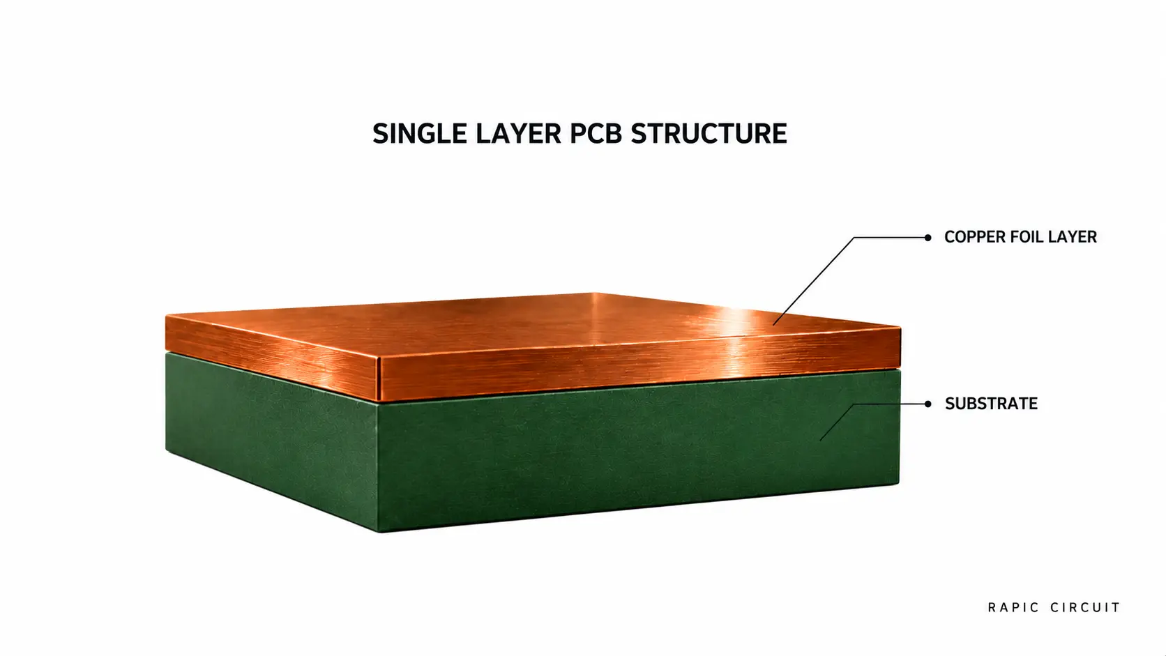
What is a Single Layer PCB?
A single layer PCB, also known as a single-sided PCB, consists of one conductive copper layer on a non-conductive substrate. It is the simplest and most cost-effective type of PCB used in electronics manufacturing.
These boards are widely used where circuit complexity is low and cost efficiency is critical.
Technical Specifications of Single Layer PCB
Material
• FR4 (standard)
• CEM-1 / CEM-3
• Aluminium-based
• FR1
• XPC
Board Thickness
• 0.4 mm to 2.4 mm
Copper Weight
• 0.5 oz
• 1 oz (standard)
• 2 oz (heavy copper optional)
Surface Finish
• HASL
• OSP
• Roller Tin
Minimum Track / Spacing
• 8/8 mil (standard)
• Tighter tolerances available on request
Minimum Hole Size
• 0.3 mm
Solder Mask Colour
• Green, White, Black, Blue, Red, Yellow
Silkscreen / Legend Marking Colour
• White, Black
Get a fast quote for your single-layer PCB requirements.
Our engineering team will review your design and provide the best solution with optimized cost and lead time.
Manufacturing & Engineering Support
• Prototype to mass production
• Panel-based production
• Quick turn fabrication
• Custom PCB design service
• Advanced PCB CAM services
• Export-grade packaging
View our complete PCB Manufacturing Capabilities
Features & Benefits
- Cost-effective for large volume production
- Simple and reliable design
- Faster manufacturing turnaround
- Easy assembly and repair
- Ideal for low-density circuits
Applications & Industries
We serve a wide range of industries where single layer PCBs are widely used, including:
• Consumer electronics
• LED lighting systems
• Power supplies
• Automotive electronics
• Industrial control systems
• Home appliances
• Prototyping and education
Pricing & Cost Factors
The cost of single layer PCB manufacturing depends on:
- Board size and complexity
- Material type
- Copper thickness
- Quantity (bulk reduces cost)
- Surface finish
- Lead time requirements
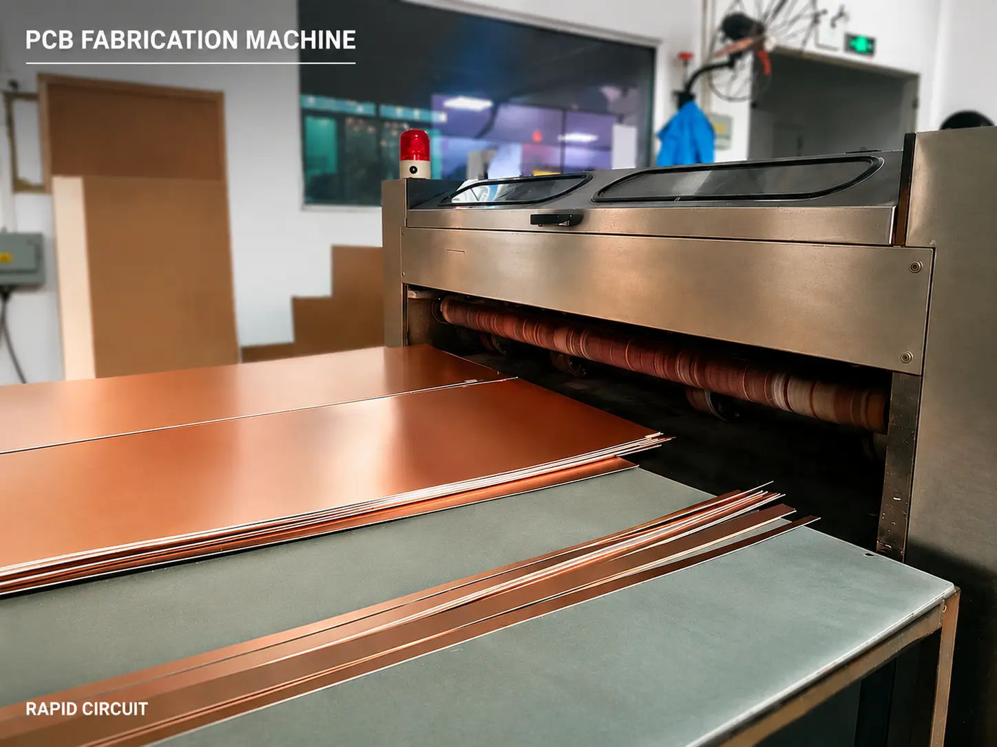
Quality & Reliability
At RAPID CIRCUIT, every PCB undergoes strict quality checks including electrical testing, visual inspection, and dimensional verification to ensure reliable performance in real-world applications.
Lead Time / Turnaround
Need a reliable PCB supplier for your next project?
Get a fast quote for your single-layer PCB requirements. Our engineering team will review your design and provide the best solution with optimized cost and lead time.
• Prototype: 24–72 hours
• Small batch: 3–5 days
• Bulk production: 7–12 days
Fast-track options available for urgent requirements.
Why Customers Choose RAPID CIRCUIT
• Fast turnaround (as low as 24 hours)
• Consistent quality across all batches
• Competitive pricing for bulk orders
• Engineering support for design optimization
• Reliable delivery across India and globally
Before full production, we recommend PCB prototyping services to validate your design and avoid costly errors.
Single Layer PCB Manufacturing Process
The single layer PCB manufacturing process involves multiple precision stages including drilling, copper imaging, etching, solder masking, testing, and final inspection to ensure reliable PCB performance.
PCB Design & Gerber File Preparation
The single layer PCB manufacturing process starts with PCB layout design and Gerber file generation for accurate circuit fabrication and production.
Copper Clad Laminate Cutting
Copper clad laminate materials such as FR4, FR1, CEM-1, CEM-3, XPC, and Aluminium sheets are cut into required production panel sizes for single layer PCB manufacturing.
CNC Drilling Process
High-precision CNC drilling machines create component holes, mounting holes, and slot openings according to PCB design data.
Copper Surface Cleaning
The copper surface is cleaned to remove oxidation, oil, dust, and contaminants before PCB imaging and etching processes.
PCB Copper Pattern Printing
PCB copper circuit patterns are printed onto the board surface using screen printing or photo imaging technology.
UV Exposure & PCB Developing
UV exposure and developing processes transfer and develop the required electrical circuit pattern on the PCB panel.
PCB Copper Etching
Unwanted copper is removed through chemical etching, leaving only the required conductive copper traces.
Resist Ink Stripping Process
Protective resist ink is removed after etching to expose the final copper circuitry on the PCB surface.
Solder Mask Coating Process
A protective solder mask layer is applied to prevent oxidation, solder bridging, and electrical short circuits.
Silkscreen Printing Process
Component markings, polarity symbols, logos, and PCB identification details are printed on the board surface.
PCB Surface Finishing
Surface finishing improves solderability and protects exposed copper pads from corrosion and environmental damage.
PCB Routing & Board Separation
Individual single-sided PCBs are separated from production panels using CNC routing or V-cut technology.
Electrical Testing Process
Electrical testing verifies PCB continuity, open circuits, short circuits, and overall electrical performance.
Final Quality Inspection
Final inspection checks PCB dimensions, drilling accuracy, solder mask alignment, and manufacturing quality standards.
PCB Packaging & Dispatch
Finished single layer PCBs are vacuum packed or moisture protected for safe shipment and delivery.
Manufacturing Flow
FAQ
What is a Single Layer PCB used for?
Single layer PCBs are used in simple electronic circuits such as LED lighting, power supplies, and consumer electronics.
What is the cost of single layer PCB manufacturing?
Costs depend on size, material, quantity, and specifications. Bulk orders significantly reduce per-unit cost.
How long does PCB manufacturing take?
Prototype boards can be delivered in 24–72 hours, while bulk production takes 7–12 days
What materials are used in single layer PCBs?
Common materials include FR4, CEM-1, and aluminium-based substrates
Can I order prototype PCBs before mass production?
Yes, prototyping is recommended to validate design before full-scale production.
What is the minimum order quantity?
MOQ varies based on requirements, but both small and large batch orders are supported.
Do you support international shipping?
Yes, PCBs can be delivered globally with secure packaging and logistics support.