Multilayer PCB Manufacturer in India
Multilayer PCB Manufacturing for Complex Electronic Applications
RAPID CIRCUIT manufactures multilayer PCBs for applications requiring higher routing density, complex layer stack-ups and compact board designs. Submit your Gerber files and fabrication requirements for engineering review and quotation.
- CAM Engineering Support
- Prototype & Production Orders
- Multilayer PCB Fabrication
- Layer Stack-Up Review
Multilayer PCB Manufacturer
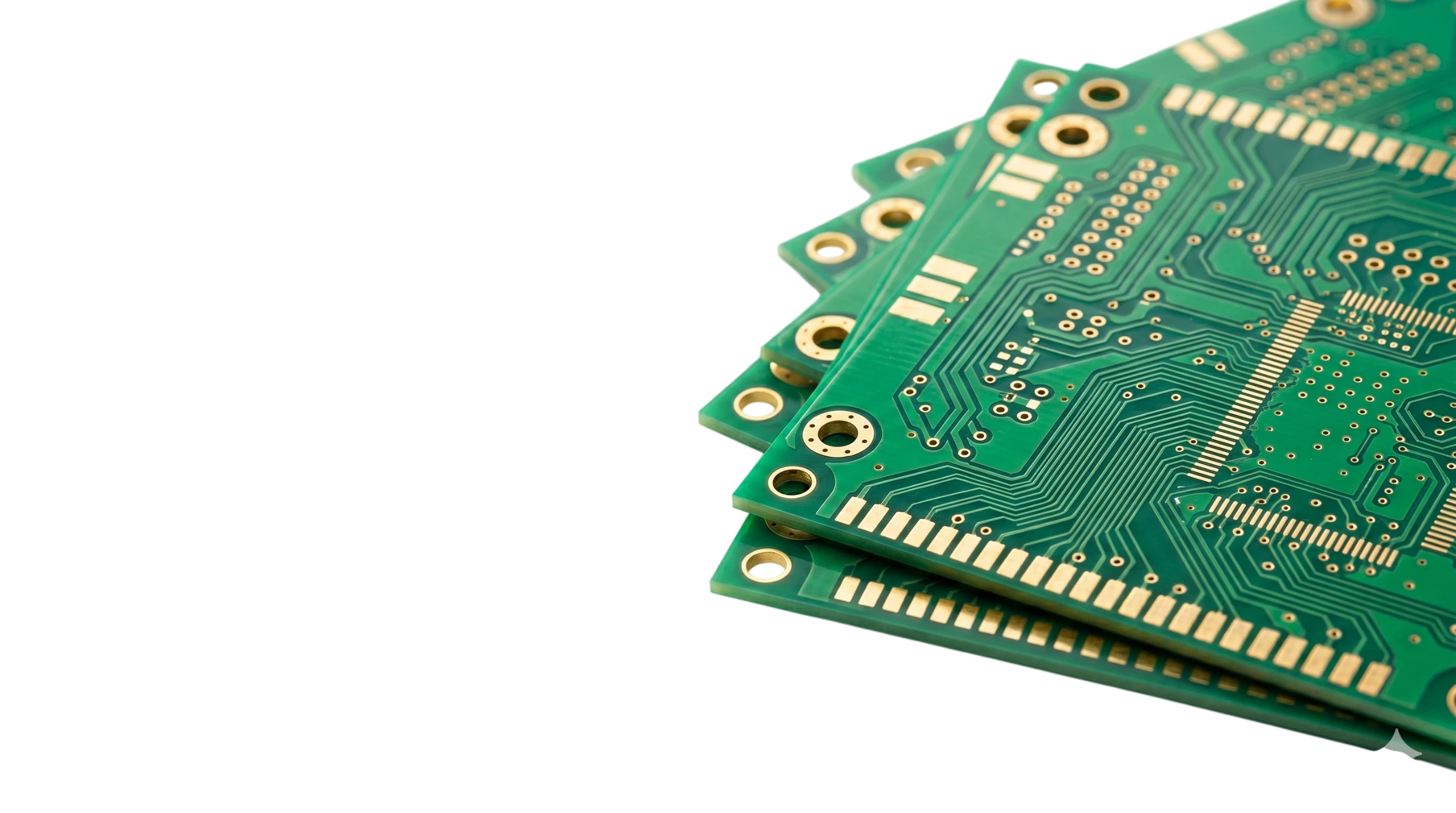
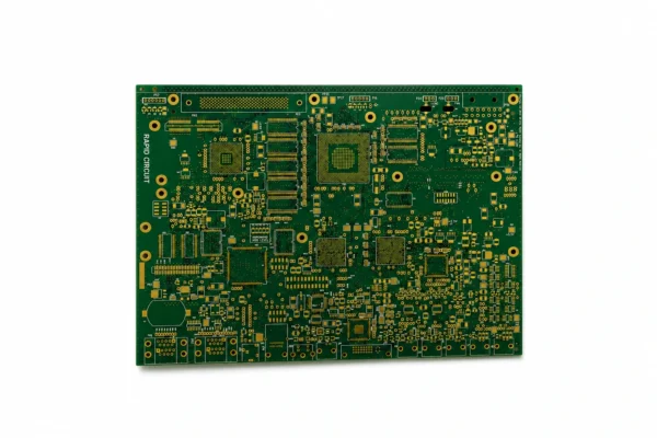
Advanced multilayer PCBs built for high-performance applications requiring complex circuitry and efficient signal management.
- High circuit density
- Enhanced performance
- Stable signal flow
Multilayer PCB Manufacturing for Complex Applications
RAPID CIRCUIT manufactures multilayer PCBs for OEMs, engineering teams and product developers requiring compact routing and multiple conductive layers. Submit your PCB fabrication data and project requirements for manufacturing review and quotation.
What is a Multilayer PCB?
A multilayer PCB consists of four or more conductive copper layers stacked and bonded together with insulating material. These layers are interconnected using plated vias, enabling highly complex circuit routing within a compact footprint. Multilayer PCBs are essential for modern electronics requiring high speed, signal integrity, and space optimization.
Multilayer PCB Technical Specifications
Material
• FR4 (standard)
• High Tg FR4
• Rogers (high-frequency applications)
Board Thickness
• 0.8 mm to 3.2 mm
Copper Weight
• 0.5 oz to 3 oz
Surface Finish
• ENIG
• HASL (lead-free)
• Immersion Silver
• Other supported finishes subject to manufacturing review
Minimum Track / Spacing
• 5/5 mil (advanced capability)
Hole & Via Requirements
• 0.2 mm (Hole and via requirements depend on the PCB stack-up and manufacturing process. Submit drill and fabrication data for engineering review.)
Available thickness depends on layer count, material and PCB stack-up. Confirm the required finished board thickness during engineering review.
Need a high-performance multilayer PCB for your project?
Send your Gerber files and fabrication requirements for manufacturing review and quotation.
Manufacturing Capabilities
• 4 to 16 layers PCB fabrication
• Multilayer PCB fabrication for prototype and production requirements
• Layer stack-up and registration review
• CAM file verification and manufacturing review
• Inner- and outer-layer process checks
• PCB lamination and drilling process
• Bare-board electrical testing

Features & Benefits
- Supports higher circuit-routing density
- Enables compact multilayer board designs
- Supports complex signal and power routing
- Suitable for applications requiring multiple conductive layers
- Can support high-speed designs when stack-up and fabrication requirements are correctly specified
Common multilayer PCB applications include:
Multilayer PCBs are widely used in:
• Telecom infrastructure
• Automotive electronics (ADAS systems)
• Medical equipment
• Aerospace systems
• Industrial automation
• Consumer electronics

Multilayer PCB Manufacturing Process
Step 1: Gerber File Submission
Gerber, drill and fabrication data are reviewed for layer stack-up and manufacturing feasibility.
Step 2: Multilayer PCB CAM Processing
Engineering checks include:
• Data Import & Gerber File Verification
• Registration & Layer Alignment
• Layer Stack-Up Verification
• Design Rule Check (DRC) for Multilayer PCB
• Drill Data Processing & Optimization
• Inner Layer Processing Checks
• Outer Layer Processing Checks
• Solder Mask & Silkscreen Verification
• Special fabrication requirement review where specified
• Panelization (PCB Array Setup)
• Copper Balancing & Thieving
• Manufacturing File Generation
• Final CAM Review & Approval

Step 3: Production
• Material Preparation (FR4 Core & Prepreg Layer Setup)
• Inner Layer Imaging (PCB Circuit Pattern Transfer)
• Inner Layer Etching (Copper Trace Formation)
• Inner Layer Inspection – AOI (Automated Optical Inspection)
• Layer Stack-Up & Lamination (Multilayer PCB Bonding Process)
• PCB Drilling Process
• Hole Metallization – Plated Through Hole (PTH) Process
• Outer Layer Imaging & Copper Plating (Circuit Build-Up)
• Outer Layer Etching (Final Copper Pattern Formation)
• Solder Mask Application
• Silkscreen Printing (Component Legend & Marking)
Step 4: Quality Control
• Electrical testing
Step 5: Delivery
PCB orders are securely packed for delivery across India and international destinations through available logistics partners.
Why Choose RAPID CIRCUIT?
Pricing & Cost Factors
Multilayer PCB cost depends on:
- Number of layers
- Material type (FR4 vs high-frequency)
- Complexity of stack-up
- Hole and via requirements
- Quantity
- Surface finish
- Testing requirements
Multilayer PCB cost depends on layer count, board construction, material, hole and via requirements, quantity, surface finish and testing requirements. Final pricing is confirmed after reviewing the fabrication data.
Engineering Review
CAM and manufacturing data are reviewed before production.
Prototype to Production Support
Support is available for prototype, small-batch and production PCB requirements.
Electrical Testing
Bare-board electrical testing is performed as part of the manufacturing process.
India & Global Delivery
PCB orders can be delivered across India and international markets.
Lead Time / Turnaround
Ready to Start Your Multilayer PCB Project?
Send your Gerber files and PCB requirements for manufacturing review and quotation by e-mail.
Multilayer PCB lead time depends on layer count, stack-up, material availability, hole and via requirements, quantity, CAM/DFM approval and current production load. The production schedule is confirmed after technical review of the manufacturing data.
Ask about expedited production availability when submitting your PCB requirements.
Explore Our PCB Solutions
FAQ
What is a multilayer PCB used for?
It is used in complex electronic systems such as telecom equipment, medical devices, and automotive electronics.
What multilayer PCB layer counts can RAPID CIRCUIT manufacture?
RAPID CIRCUIT manufactures multilayer PCBs from 4 to 16 layers, depending on the design, material, board thickness, and technical requirements. Please share your Gerber files and specifications for feasibility review and quotation.
What is the cost of multilayer PCB manufacturing?
Multilayer PCB cost depends on layer count, material, board dimensions, thickness, copper requirements, hole and via requirements, surface finish, testing, quantity and production schedule. Submit your fabrication data for an accurate quotation.
What is the difference between double layer and multilayer PCB?
A double-layer PCB has two conductive layers, while a multilayer PCB has Four or more conductive layers bonded into a single board structure. Multilayer construction supports more complex routing and higher circuit density.
How long does fabrication take?
Lead time depends on the PCB layer count, stack-up, material, quantity, fabrication requirements and current production load. The confirmed production schedule is provided after engineering review.
What materials are used?
FR4 and supported high-frequency PCB materials are available depending on the required stack-up and application. Submit your material requirement for confirmation during manufacturing review.
Can I order prototype multilayer PCBs?
Yes. Multilayer PCB prototypes can be manufactured before proceeding to larger production quantities.
What information should I send for a multilayer PCB quotation?
Send your Gerber files or available PCB manufacturing data together with the required quantity, board dimensions, layer count, material, finished thickness, copper thickness, surface finish and delivery requirements. Include any special fabrication or testing requirements that apply to the project.